
:quality(85):upscale()/2025/03/11/034/n/1922153/2d2e63c567d0cc04d4abd6.11200800_.png)
:quality(85):upscale()/2025/03/11/969/n/1922729/7cde8e8867d0b5ffa653e8.91714986_.jpg)
:quality(85):upscale()/2025/03/11/840/n/1922153/22e2b18867d08ab78a0f25.15915796_.jpg)
:quality(85):upscale()/2025/03/11/676/n/1922153/b931932167d0532f185102.18386880_.jpg)


Chinese university designed 'world's first silicon-free 2D GAAFET transistor,' claims new bismuth-based tech is both the fastest and lowest-power transistor yet

A research team from Peking University has published its findings on a two-dimensional, low-power GAAFET transistor, the first of its kind in the world. Led by Professor Peng Hailin and Qiu Chenguang, the multi-disciplinary team published in Nature, with some team members calling the discovery nothing short of a monumental breakthrough.
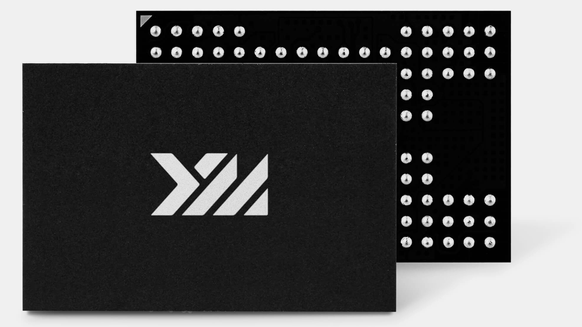
The Peking team has fabricated what the paper describes as a "wafer-scale multi-layer-stacked single-crystalline 2D GAA configuration."
"It is the fastest, most efficient transistor ever", said Peng of his team's new transistor. “If chip innovations based on existing materials are considered a ‘short cut, ’ then our development of 2D material-based transistors is akin to ‘changing lanes, ’” continues Peng in a statement for Peking University's website (accessed via South China Morning Post).
The team claims to have tested their transistor against products from Intel, TSMC, Samsung, and elsewhere, where it outperformed them under matching operating conditions.
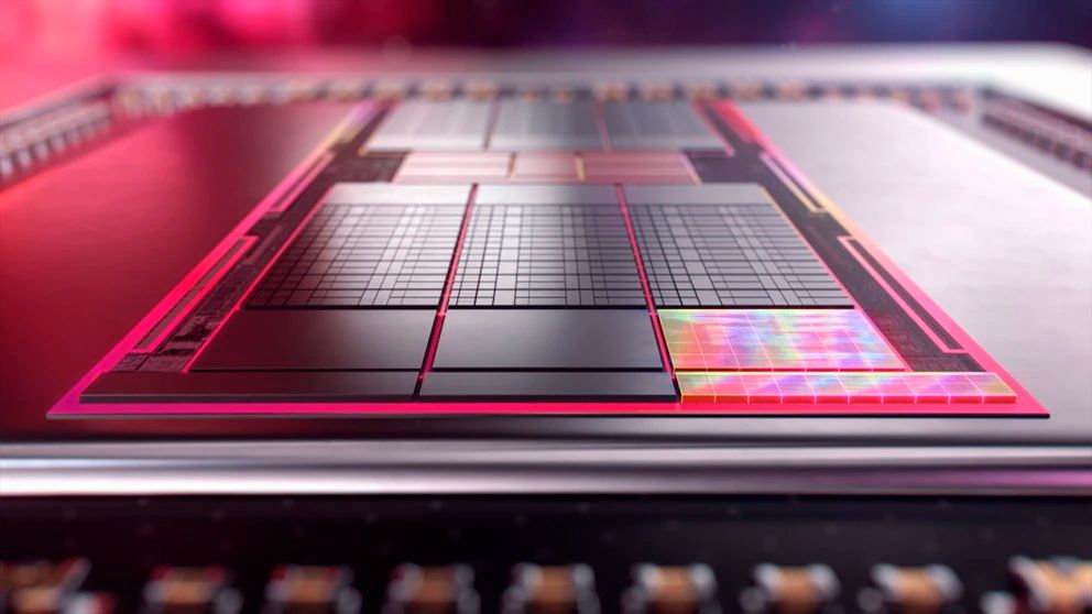
To break down the technobabble, we must start with GAAFET. Gate-all-around field-effect transistors, GAAFET for short, are the next evolution of transistor technology after MOSFETs and FINFETs.
Innovation in transistors has largely been driven by better control of sources and gates communication; MOSFETs have a source touched on one plane by a gate, FINFETs have three planes touch their gates, where gate-all-around surrounds sources in their intersecting gates, as the name would imply. Below is Samsung's illustrative diagram on the differences (plus Samsung's proprietary MBCFET version of GAAFET).
GAAFET transistors are nothing new; the transistor technology is essential for fabricating microchips at 3nm and below. Peking's major innovation comes from the two-dimensional nature of their transistors, facilitated by using an element other than silicon.
Get Tom's Hardware's best news and in-depth reviews, straight to your inbox.
Bi₂O₂Se, or bismuth oxyselenide, is a semiconductor material studied for its use in sub-1nm process nodes for years, largely thanks to its ability to be a 2D semiconductor. Two-dimensional semiconductors, like 2D Bi₂O₂Se, are more flexible and sturdy at a small scale than silicon, which runs into reduced carrier mobility at even the 10nm node.
The Odyssey from Silicon To Bismuth
Such breakthroughs into stacked 2D transistors and the move from silicon to bismuth are exciting for the future of semiconductors and are necessary for the Chinese industry to compete on the leading edge of semiconductors.
Thanks to a U.S.-China trade war over chips and modern technology, China finds itself cut off from tools like EUV lithography that enable the production of processors on nodes that the rest of the tech world has been producing for nearly a decade. As a result, China has invested heavily in research that will allow it to leapfrog the current state of the tech industry, not content to catch up merely.
While 2D GAAFET transistors may not be the future of semiconductor fabrication, the study represents burgeoning young minds in China prepared to innovate on what is possible to push the industry forward. As the United States stands ready to ramp up its trade embargoes and restrictions against China's tech access, including a potential ban on GAAFET technology, China's tech industry is racing against the clock of warring empires.
What's Your Reaction?
 Like
0
Like
0
 Dislike
0
Dislike
0
 Love
0
Love
0
 Funny
0
Funny
0
 Angry
0
Angry
0
 Sad
0
Sad
0
 Wow
0
Wow
0