


:quality(85):upscale()/2025/11/10/782/n/49351757/8170ecd6691224df8bd1d7.49547606_.png)
:quality(85):upscale()/2025/11/21/894/n/24155406/f08298fe6920cb78a61ca3.64427622_.jpg)
:quality(85):upscale()/2025/10/31/699/n/24155406/907a28006904d9f5870b34.67078517_.png)
:quality(85):upscale()/2025/11/26/724/n/1922153/364868b6692729990f9002.05869709_.png)


Samsung touts 96% lower-power NAND design — researchers investigate design based on ferroelectric transistors
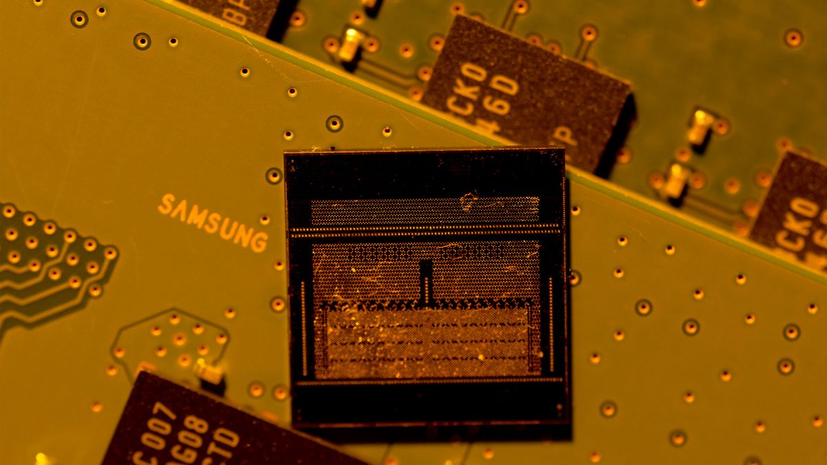
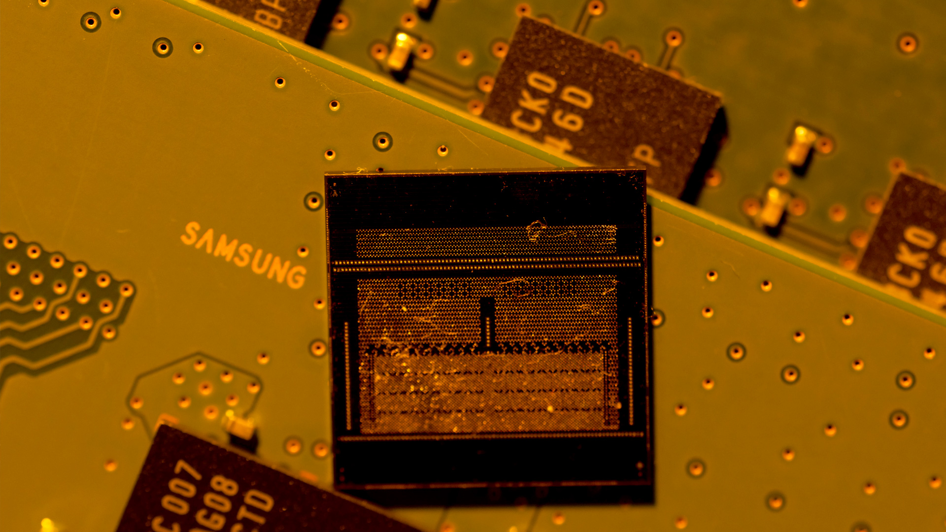
Samsung researchers have published a detailed account of an experimental NAND architecture that aims to cut one of the technology’s largest power drains by as much as 96%.
The work — Ferroelectric transistor for low-power NAND flash memory — was carried out by researchers at the Samsung Advanced Institute of Technology and appears in the journal Nature. It describes a ferroelectric field-effect transistor (FeFET) design intended for future 3D NAND, combining a hafnia-based ferroelectric with an oxide-semiconductor channel and introducing a near-zero pass-voltage operation that forms the basis of the 96% power reduction figure.
The experiments also cover retention and cycling limits. In planar form, the ferroelectric cells support a wide memory window and demonstrate five-level programming, although endurance at that density is modest. A PLC-class configuration holds for a few hundred cycles, while QLC-equivalent use approaches a thousand at both room temperature and 85 °C. The authors note that further development of program-inhibit schemes and negative-voltage generation will be required before a full 3D array could be qualified for production. They also point out that the oxide channel’s behaviour under high-temperature stress remains a key area for follow-up work.
Get Tom's Hardware's best news and in-depth reviews, straight to your inbox.

Follow Tom's Hardware on Google News, or add us as a preferred source, to get our latest news, analysis, & reviews in your feeds.
Luke James is a freelance writer and journalist. Although his background is in legal, he has a personal interest in all things tech, especially hardware and microelectronics, and anything regulatory.
What's Your Reaction?
 Like
0
Like
0
 Dislike
0
Dislike
0
 Love
0
Love
0
 Funny
0
Funny
0
 Angry
0
Angry
0
 Sad
0
Sad
0
 Wow
0
Wow
0