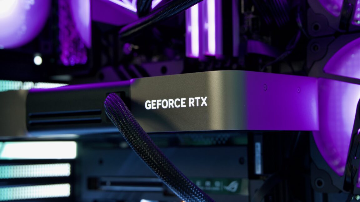


Jensen Huang anticipates 20% performance boost from gate-all-around transistors

Serving tech enthusiasts for over 25 years.
TechSpot means tech analysis and advice you can trust.
In brief: While covering a wide range of topics during his keynote at Nvidia's GTC, CEO Jensen Huang briefly touched on the company's GPU roadmap beyond the upcoming Rubin architecture. The Feynman generation and those that follow will likely adopt semiconductor nodes featuring gate-all-around (GAA) transistors – the next evolution in transistor technology after FinFET.
During a Q&A session at the GPU Technology Conference, Huang estimated a roughly 20% performance uplift from transitioning to GAA architecture. His comments offer an early indication of the company's expectations for future graphics chip designs.
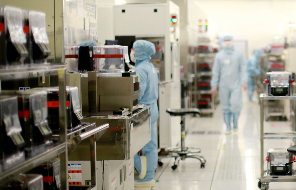
Semiconductor manufacturers such as TSMC and Intel have touted GAA transistors as a key technology for process nodes beyond 3nm. Recent nodes, including 3nm, have employed FinFET, a structure where the transistor gate surrounds the current channel on three sides. However, as bleeding-edge transistors shrink and become more densely packed in advanced nodes, electrical leakage becomes a growing concern.
Also see: How CPUs are built, the design process – touches on the basics of how transistors work
GAA addresses this issue by stacking current channels vertically, increasing the total channel area while allowing gates to surround the channels on all four sides. Although the technique is more expensive, it enhances both performance and energy efficiency.
Intel's upcoming 18A node will introduce GAA with Panther Lake laptop CPUs and Clearwater Forest server processors later this year. TSMC plans to adopt GAA for its 2nm N2 process, which is nearing production and is expected to debut in the iPhone 18 Pro's A20 SoC in late 2026.
At GTC, Huang officially revealed Nvidia's next GPU generation, Vera Rubin, which will be built on TSMC's N3 node and is expected to become available to enterprise clients next year. He also shared early details about Rubin's successor, Feynman, which is anticipated to arrive in 2028.
Although information on Feynman's semiconductor process is forthcoming, it's likely to utilize a 2nm-class node, though Nvidia may also consider Intel's 18A. In either case, GAA will be a key component. Huang remarked that while a 20% performance boost from GAA isn't revolutionary, "we'll take what we can get."
Meanwhile, backside power delivery is emerging as another critical technology for sub-3nm nodes. TSMC is not expected to implement it until the following node called A16 beginning 2026, whereas Intel will introduce its version with 18A later this year.
Interestingly, during the GTC Q&A, Huang also described Nvidia as an "AI infrastructure company." While Nvidia rose to prominence for its gaming GPUs, the AI boom has propelled the value of its enterprise division into the multi-trillion-dollar range.

What's Your Reaction?
 Like
0
Like
0
 Dislike
0
Dislike
0
 Love
0
Love
0
 Funny
0
Funny
0
 Angry
0
Angry
0
 Sad
0
Sad
0
 Wow
0
Wow
0