


:quality(85):upscale()/2025/11/10/782/n/49351757/8170ecd6691224df8bd1d7.49547606_.png)
:quality(85):upscale()/2025/11/21/894/n/24155406/f08298fe6920cb78a61ca3.64427622_.jpg)
:quality(85):upscale()/2025/10/31/699/n/24155406/907a28006904d9f5870b34.67078517_.png)
:quality(85):upscale()/2025/11/26/724/n/1922153/364868b6692729990f9002.05869709_.png)


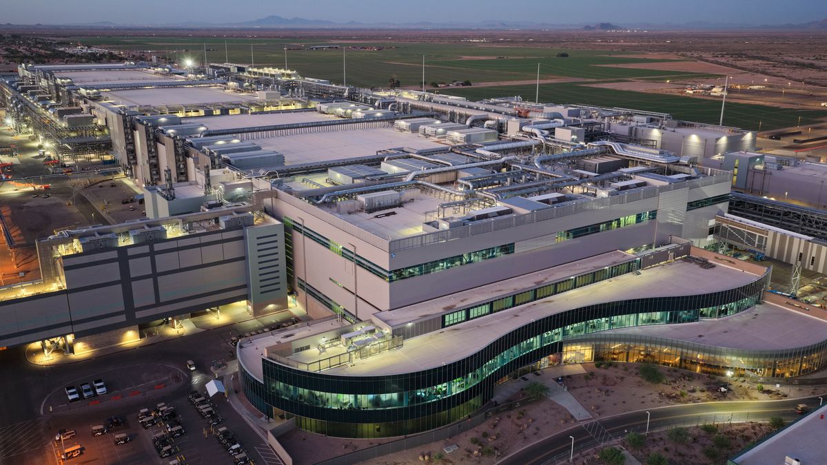
Intel's Fab 52 is bigger and better equipped than TSMC's Arizona facilities — Intel's production volume dwarfs TSMC's operations in the U.S.

Tom's Hardware Premium Roadmaps
Intel is trying to catch up with TSMC in terms of process technologies and advanced global production capacity, but when it comes to the U.S., the chip giant remains unrivalled. Intel's Fab 52 is more advanced than TSMC's current Fab 21 phase 1 and upcoming Fab 21 phase 2 facilities and its production capacity is comparable to both modules combined, according to a report by CNBC.
At present, Fab 52 is equipped with four ASML Twinscan NXE Low-NA EUV lithography systems (as observed by @IntelProMUltra), including at least one NXE:3800E — ASML's most advanced Low-NA EUV machine that borrows wafer handler, faster wafer stages, and light source from next-generation High-NA EUV tools and therefore can process up to 220 wafers per hour at a 30 mJ/cm^2 dose. The plant also has three NXE:3600D systems, which can process 160 wafers per hour at a 30 mJ/cm^2 dose.
In total, there will be at least 15 EUV scanners at Intel's Silicon Desert campus in Ocotillo, Arizona. However, we can only wonder how many of them will be High-NA EUV lithography tools and how many will be installed in the upcoming Fab 62. In any case, the words 'at least' imply that Intel has enough space to install more than 15 EUV lithography machines at its Arizona facilities.
When compared to TSMC's Fab 21 phase 1 (which produces chips on the company's N4 and N5 process technologies), Intel's Fab 52 can make chips on considerably more advanced nodes (down to 1.8nm-class and beyond), and it can process two times more wafers per month. In fact, given that TSMC tends to build fab modules with production capacity of around 20,000 WSPM, even when TSMC completes its N3-capable Fab 21 phase 2, Intel's Fab 52 will remain on par or even a bit ahead of TSMC's facilities in Arizona when all three are fully ramped.
In fact, given that Intel's 18A production node is considerably more sophisticated than TSMC's N4 or N4P, the straightforward comparison of production capacities is not completely accurate, as Intel's fab has to do more work to create the node (even using the more advanced Twinscan NXE:3800B).
There is a caveat regarding Intel's Fab 52 ramp schedule, however. At present, it is ramping up production of Intel's Panther Lake processors using 18A technology, which is still in an early stage of its yield curve. Intel expects 18A yields to reach world-class levels in early 2027. Before then, Intel will not increase production of CPUs on this node beyond a certain level, so the fab will now be fully utilized, and some portion of its production capacity will remain unused. By contrast, TSMC ramps chip production using proven process technologies in the U.S., enabling rapid ramp-up and a quick increase in fab utilization to near 100%.
Get Tom's Hardware's best news and in-depth reviews, straight to your inbox.
*Note that there are more than four weeks in an average month, so the maximum capacity of Intel's Fab 52 when fully ramped can be higher than 40,000 WSPM, depending on factors like planned maintenance and unplanned downtime.

Follow Tom's Hardware on Google News, or add us as a preferred source, to get our latest news, analysis, & reviews in your feeds.
Anton Shilov is a contributing writer at Tom’s Hardware. Over the past couple of decades, he has covered everything from CPUs and GPUs to supercomputers and from modern process technologies and latest fab tools to high-tech industry trends.
What's Your Reaction?
 Like
0
Like
0
 Dislike
0
Dislike
0
 Love
0
Love
0
 Funny
0
Funny
0
 Angry
0
Angry
0
 Sad
0
Sad
0
 Wow
0
Wow
0