

:quality(85):upscale()/2025/11/10/782/n/49351757/8170ecd6691224df8bd1d7.49547606_.png)
:quality(85):upscale()/2025/11/21/894/n/24155406/f08298fe6920cb78a61ca3.64427622_.jpg)
:quality(85):upscale()/2025/10/31/699/n/24155406/907a28006904d9f5870b34.67078517_.png)
:quality(85):upscale()/2025/11/26/724/n/1922153/364868b6692729990f9002.05869709_.png)


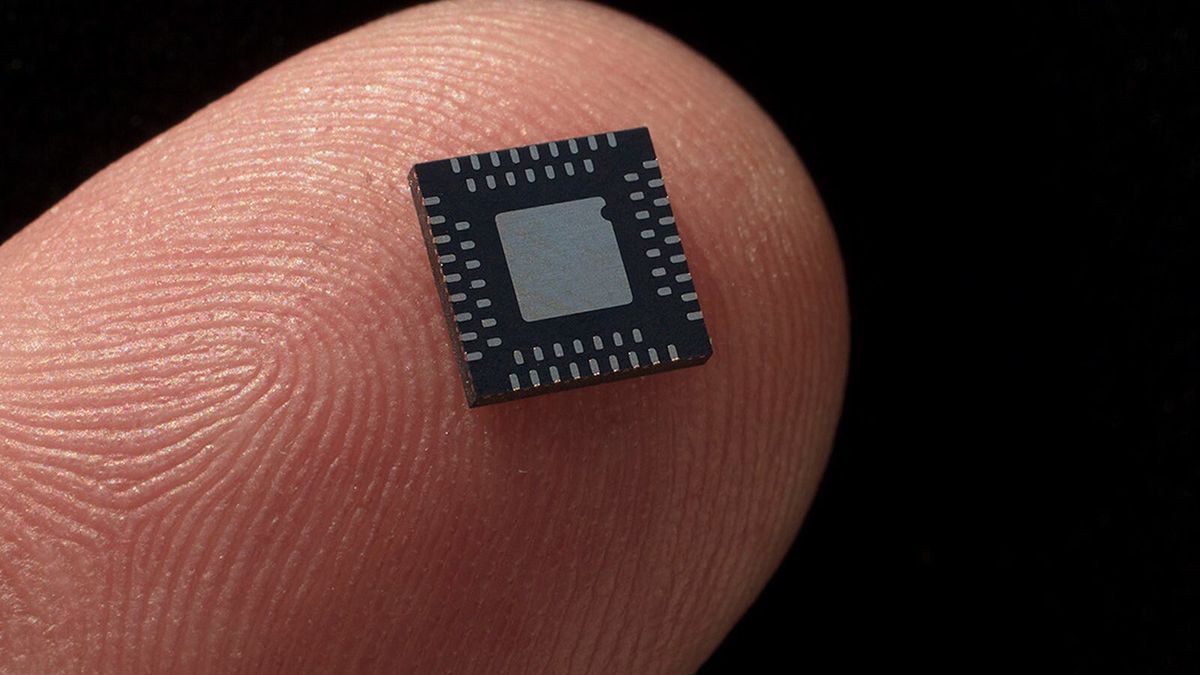
China may have reverse engineered EUV lithography tool in covert lab, report claims — employees given fake IDs to avoid secret project being detected, prototypes expected in 2028
A secret laboratory in China has quietly assembled a prototype extreme ultraviolet (EUV) lithography system and is now testing it stealthily, which means that the country may be close to replicating the most advanced technology that currently exists on Earth, reports Reuters.
The tool was reportedly developed by reverse engineering existing scanners from ASML and is said to be on-track to make prototype chips in 2028. If the information is correct, then Chinese scientists have made numerous breakthroughs across multiple disciplines in just a few years instead of decades, a scenario that appears extremely unlikely. Further analysis of the report indicates that China's laboratory is far from completing the tool, meaning that the country is years away from making chips using EUV lithography.
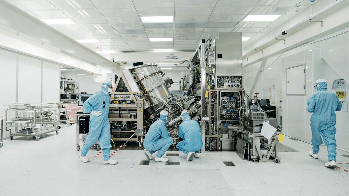
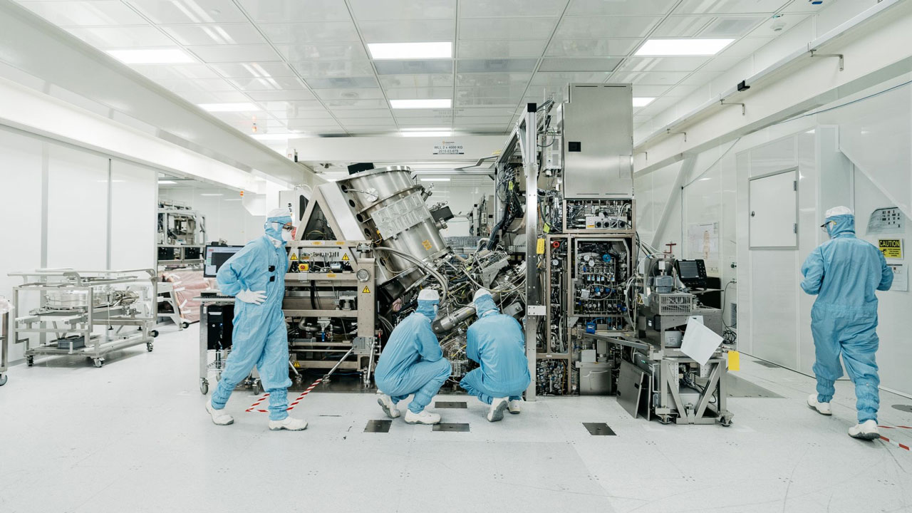
China's alleged EUV scanner
The system was reportedly completed in early 2025 inside a highly secured facility in Shenzhen and occupies nearly an entire factory floor. The Chinese machine reportedly generates EUV light with a wavelength of 13.5nm using the same laser-produced plasma (LPP) method as ASML Twinscan NXE machines, not the particle accelerator-based steady-state microbunching (SSMB) method designed at Tsinghua University or discharge-produced plasma (DPP) technology developed at Harbin Institute of Technology (HIT), which might prove the point that the system was reverse-engineered or at least contains a substantial amount of technologies pioneered by ASML.
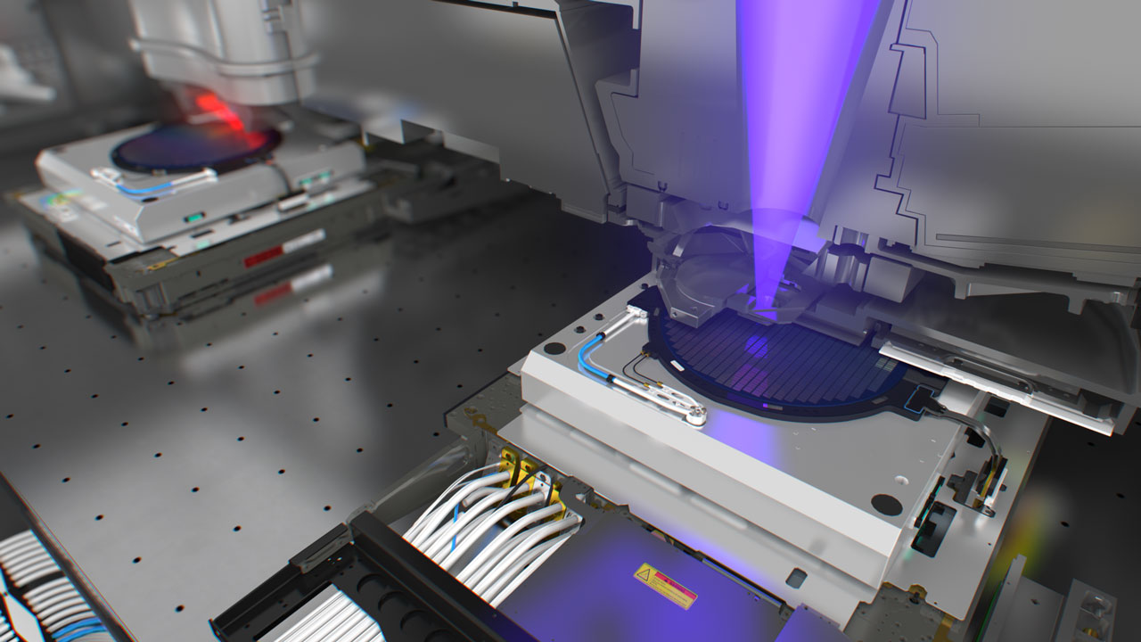
ASML's laser-produced plasma (LPP) method uses tiny molten tin droplets, roughly 25–30 microns in diameter, which are injected into a vacuum chamber at a rate of about 50,000 droplets per second. Then, a high-power CO₂ laser first fires a low-intensity pre-pulse at each droplet, flattening it into a disk-like shape, followed by a more powerful main pulse that vaporizes the flattened tin and creates a superheated plasma with temperatures exceeding 200,000°C. This plasma emits isotropic EUV light, which is then collected by a large multilayer collector mirror and directed into the lithography system's reflective optics for patterning silicon wafers. This process repeats tens of thousands of times per second.
The machine is reportedly larger than the original, but it is operational in the sense that it can generate EUV radiation. However, it has not progressed to make usable chips as it still struggles to replicate 'the precision optical systems' features by Twinscan NXE systems. Furthermore, there is no word about power of the EUV light source, a crucial parameter that defines whether a tool can or cannot be used for volume production.
Not operational, for now
The report clearly states that the Chinese EUV scanner cannot currently be used to make chips, but the Chinese government reportedly wants the first chip prototypes to emerge in 2028, two or three years down the road. However, a more realistic target is 2030, four or five years from now, which is a long time. Meanwhile, from the report, it is not completely clear what stage the Chinese team is at today.
The report does not disclose which specific components of the optical system are the primary bottlenecks, as the article groups them rather generally. In particular, it is uncertain if the alleged EUV tool struggles to replicate the ultra-precise collector mirror system coated with multilayer molybdenum-silicon (Mo/Si) stacks, illuminator optics (which shapes and uniforms the beam using faceted mirrors), or projection optics (a series of aspheric mirrors for 4X – 8X reduction imaging with sub-nanometer wavefront errors). ASML outsources the development and production of these components to Carl Zeiss from Germany. If the developers failed to replicate the collector itself, then the rest of the machine can hardly be called an EUV lithography system, as technically, the only thing they have is some kind of light source that they have yet to learn how to use. Yet, even if the developers cannot replicate illuminator optics or projection optics (suggesting that the collector itself is there), it still means they do not have even a poorly working EUV lithography tool, but rather a set of certain components.
Get Tom's Hardware's best news and in-depth reviews, straight to your inbox.
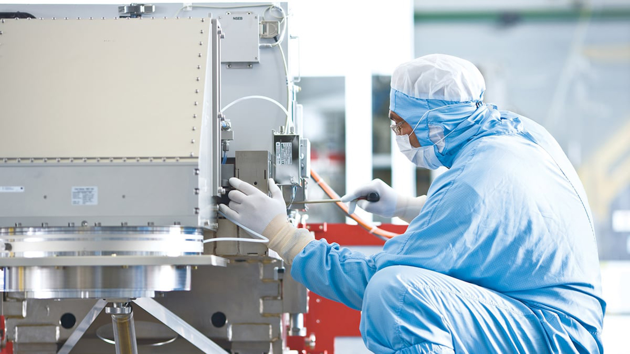
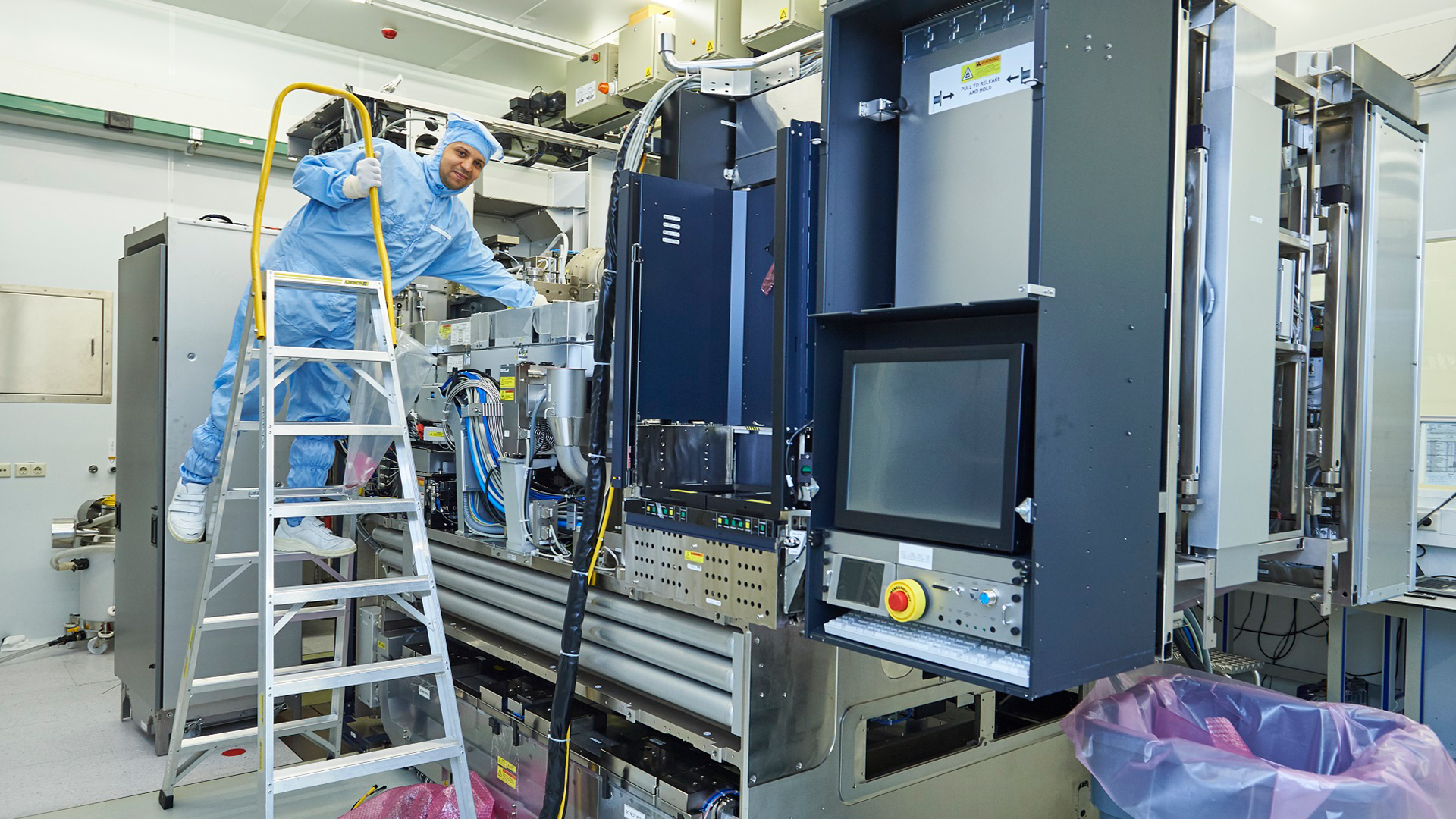
When talking about advanced lithography equipment, we must keep in mind that such tools rely on seamless integration of sophisticated light sources, advanced optics, ultra-precise mechanical engineering, complex control software, and specialized materials, all of which must function reliably within nanometer-scale tolerances demanded by modern chip manufacturing. The story has no word about the state of the mechanical systems of the alleged tool: we know nothing about the wafer stocker system, wafer stages, or reticle stages, all of which are crucial for operation and yields.
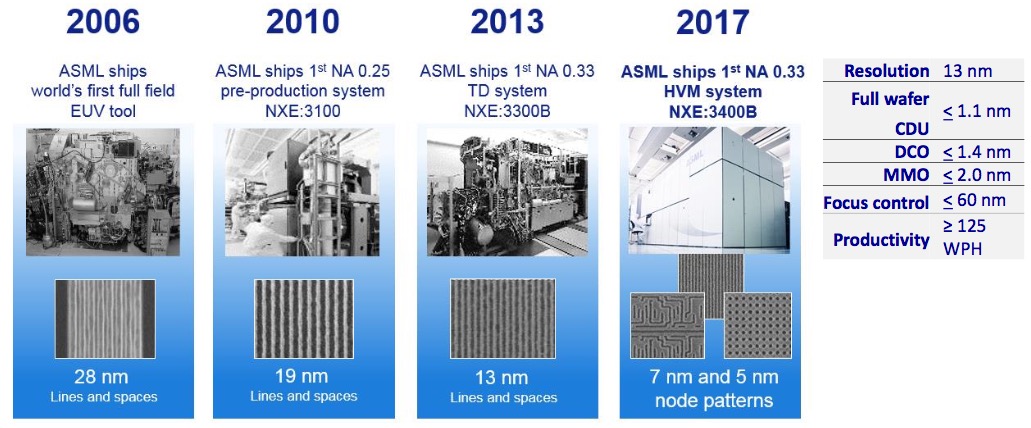
To put China's EUV efforts into perspective, the secret lab is not even close to building an alpha tool. For now, what the Chinese lab has cannot even put the light on a wafer, save for printing lines and spaces, something ASML's tool could do in 2006, about 11 years before the company shipped its first Twinscan NXE:3400B system meant for high-volume manufacturing. Of course, reverse engineering certain components can give Chinese engineers a speed boost, but it remains to be seen how significant this one is going to be.
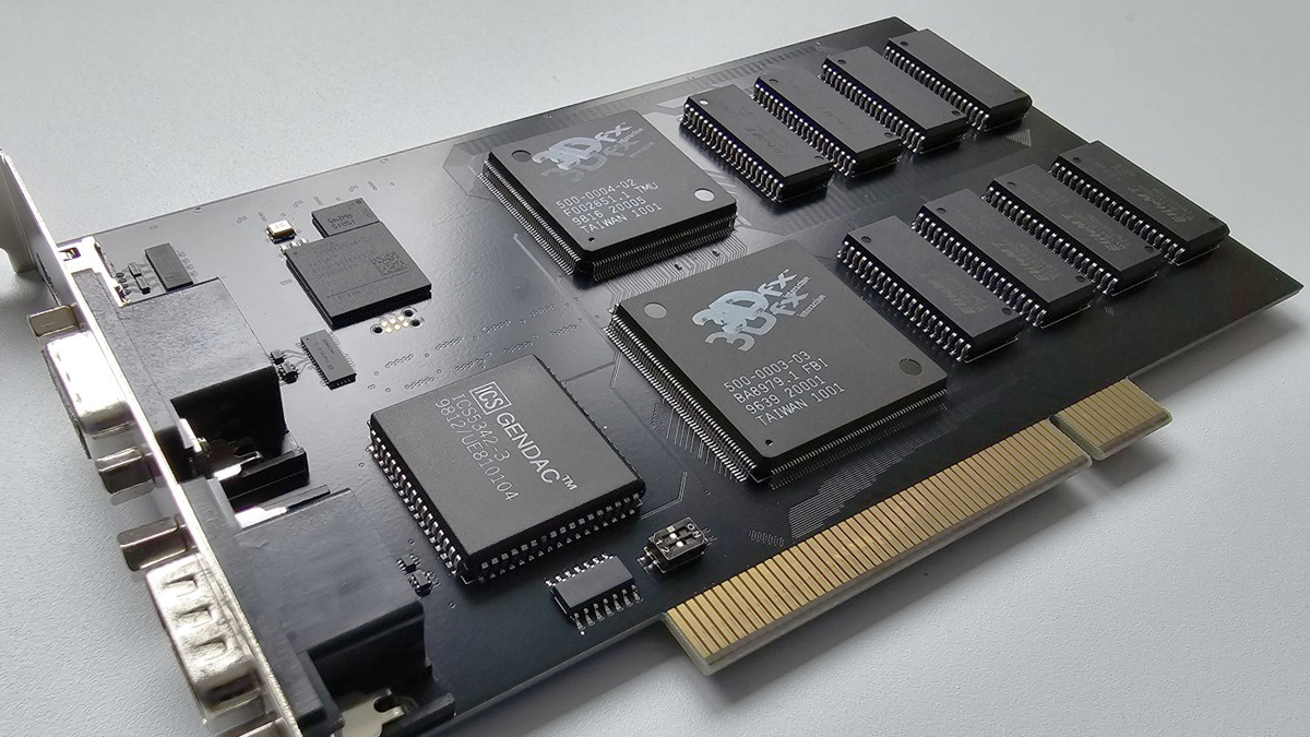
Reverse engineering an ASML Twinscan NXE?
According to Reuters's sources familiar with the effort, the Chinese EUV tool was 'developed' by a team that includes former engineers from ASML and recent university graduates, who allegedly reverse-engineered the company's EUV machines. The secret lab was so stealthy that its employees were given fake IDs to avoid detection of their concentration in one place by foreign spies.
Yet, it is unclear how any engineers from China could reverse engineer an EUV lithography scanner, as the Dutch company has never supplied one to China and hardly taught personnel from China how to service its EUV systems that are not allowed to be shipped to the People's Republic.
Reverse engineering a machine that contains over 100,000 parts is a hard task that takes hundreds of engineers with knowledge of the matter, which is why the secret entity led by the Government of China hired not only former engineers from ASML China, but also former employees of the Dutch company from elsewhere, presumably from Europe, Taiwan, and the U.S. For example, Lin Nan, formerly responsible for EUV light source technology at ASML, now leads a team at the Chinese Academy of Sciences’ Shanghai Institute of Optics that has filed eight EUV-related patents in just 18 months. Yet, this may mean that he uses his experience and knowledge rather than trying to replicate what he did at ASML or reverse engineer what he did at ASML due to the absence of an EUV scanner in his lab.
“It makes sense that companies would want to replicate our technology, but doing so is no small feat,” a statement by ASML published by Reuters reads.
The report says that around 100 recent university graduates are tasked with reverse-engineering parts from EUV and DUV lithography tools, with each workplace monitored by a dedicated camera that records the disassembly and reassembly process, an important part of the whole China's lithography program, according to the report. Employees who successfully put components back together receive bonuses. Yet again, a Twinscan NXE tool is a mechanism consisting of over 100,000 parts working together, not just a sum of all parts.
To sum up, China has reportedly built a secret prototype EUV lithography system and begun testing it, which suggests that the country may be closer to reproducing the most advanced chipmaking technology in existence than previously believed. However, details provided by the report indicate that China is still years — if not a decade — away from making chips using EUV lithography.
The machine can generate 13.5-nm EUV light using the same laser-produced plasma (LPP) method employed by ASML, which may demonstrate extensive reverse engineering of Western technology rather than the use of alternative domestic approaches. However, the tool is significantly larger than commercial systems available today, it cannot produce usable chips, and appears to struggle with other elements of EUV lithography, particularly ultra-precise optics supplied to ASML by Carl Zeiss. In fact, details about the system like light source power, optical subsystem maturity, and the state of critical mechanical components remain unclear.
While China expects first prototype EUV chips to emerge in 2028, Reuters's sources suggest 2030 is more realistic. Yet, the whole effort relies heavily on recruiting former ASML engineers and reverse engineering parts from existing EUV and DUV tools, which are not only hard to develop, but are extremely hard to make. Meanwhile, there is no word whether the current team responsible for disassembling and reassembling components can actually make an ultra-complex machine consisting of over 100,000 parts work flawlessly to produce semiconductors in high volumes.

Follow Tom's Hardware on Google News, or add us as a preferred source, to get our latest news, analysis, & reviews in your feeds.
Anton Shilov is a contributing writer at Tom’s Hardware. Over the past couple of decades, he has covered everything from CPUs and GPUs to supercomputers and from modern process technologies and latest fab tools to high-tech industry trends.
What's Your Reaction?
 Like
0
Like
0
 Dislike
0
Dislike
0
 Love
0
Love
0
 Funny
0
Funny
0
 Angry
0
Angry
0
 Sad
0
Sad
0
 Wow
0
Wow
0